Top Semiconductor Packaging Giants: Where Chip Innovation Meets Industrial Engineering
Top Semiconductor Packaging Giants: Where Chip Innovation Meets Industrial Engineering
In the quiet backbone of the global electronics supply chain, semiconductor packaging companies play a pivotal role—transforming delicate silicon dies into rugged, reliable components ready for integration into smartphones, AI accelerators, and automotive systems. These firms are the unsung architects of modern technology, where precision, miniaturization, and performance convergence define success. From Japanese master architects to U.S.-led innovators and European specialists, a select group of packaging powerhouses deliver the critical interface between microscopic chips and the devices shaping daily life.
With data from recent market analyses and industry reports, this article maps the landscape of leading semiconductor packaging providers, their core technologies, regional strengths, and the invisible yet indispensable impact they wield across industries.
The Pillars of Modern Semiconductor Packaging
Semiconductor packaging is far more than protective casing—it serves as a bridge between chip fabrication and end-use application. Key functions include thermal management, electrical signal routing, mechanical durability, and advanced material integration.As device architectures grow complex—with 3D stacking, embedded memory, and heterogeneous integration—the demand for cutting-edge packaging solutions has surged. The industry’s evolution is driven by several core technological pillars: - **Fan-out Wafer-Level Packaging (FOWLP)**: Enables fine-line interconnects while reducing form factor and improving performance. - **2.5D/3D Integration**: Stacking dies vertically or laterally to boost bandwidth and reduce latency, critical for AI and high-performance computing.
- **Advanced Thermal Solutions**: Including temperature-aware substrates and embedded heat spreaders to manage increasing power densities. - **Heterogeneous Integration**: Combining logic, memory, sensors, and RF components into single packages for system-on-chip (SoC) dominance. “Packaging today isn’t just about protection—it’s about enabling functionality,” notes Dr.
Sarah Lin, Senior Analyst at MarketsandMarkets. “These technologies unlock capabilities that silicon fabrication alone cannot deliver, making them essential to next-generation electronics.”
Global Leaders Shaping the Semiconductor Packaging Landscape
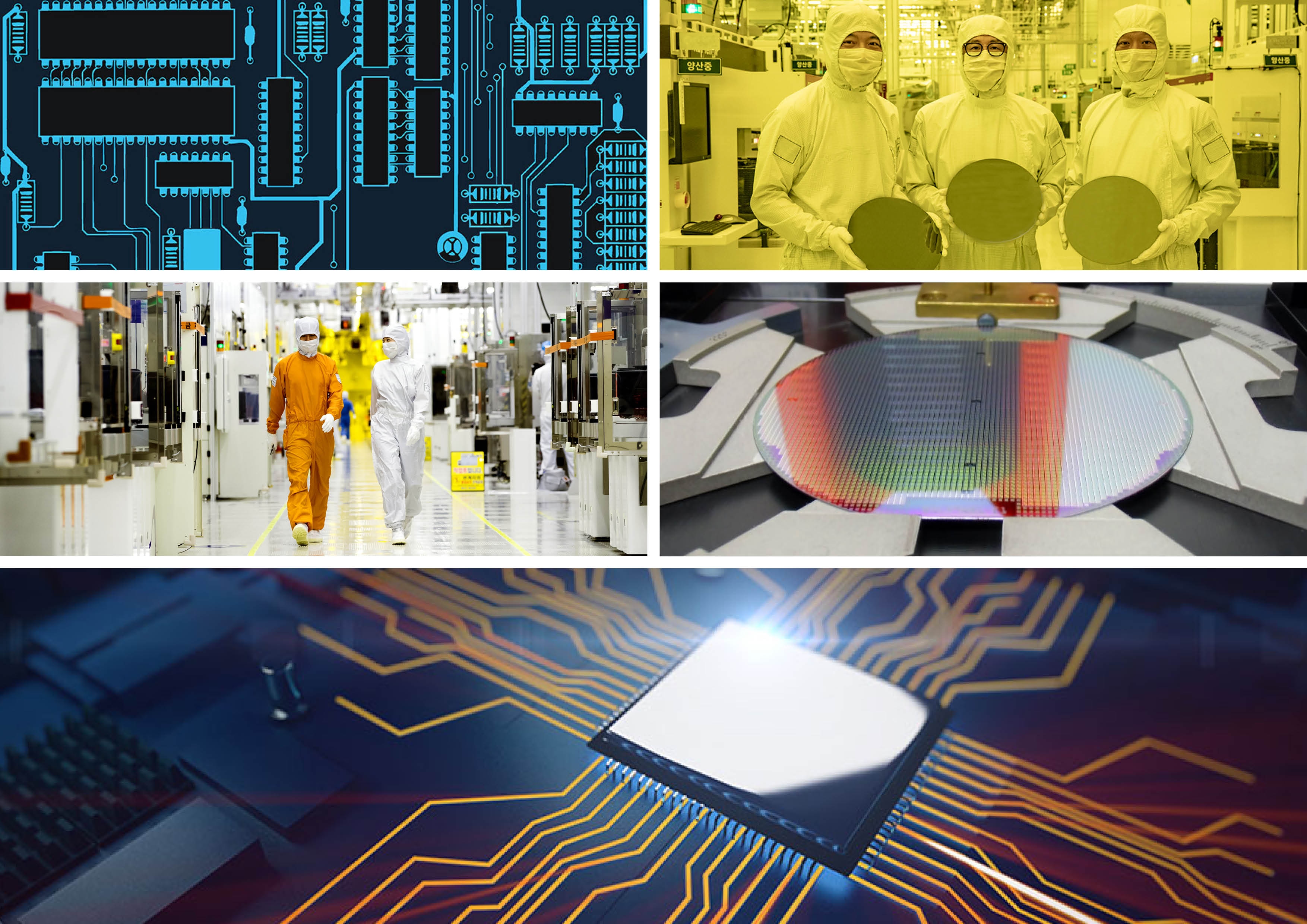
> The top semiconductor packaging firms worldwide combine deep technical expertise with strategic scale, positioning themselves at the edge of what chips can physically achieve. Benchmarking against business size, R&D investment, and customer diversity, the following companies stand out as industry architects: **ASML’s Ecosystem Partners & Subsystems Providers (Japan & Taiwan)** While ASML dominates lithography, Japanese and Taiwanese partners like Tokyo Electron (TEL) and ASE Group lead in advanced packaging.TEL delivers high-precision deposition and etch tools essential for fan-out and fan-in FOWLP processes, supporting clients from Apple to NVIDIA. ASE, headquartered in Taiwan, is the world’s largest EMS (electronics manufacturing services) provider, specializing in advanced TSV (Through-silicon Via) stacking and system-in-package (SiP) integration for mobile and IoT devices. **NTT DENSO & Sumitomo Electric (Japan)** Leveraging Japan’s precision engineering tradition, these firms excel in multi-chip modules (MCMs) and power management packaging.
Their innovations in substrate materials and miniaturized interconnects support the rising demand for compact, energy-efficient automotive and industrial electronics. **AMD-backed Packaging Innovators (U.S.)** While not a traditional manufacturer, AMD’s strategic collaborations with U.S. packaging leaders—including Flex Logistics and emergency pandemic-inspired vertical integrations—highlight a shift toward proprietary packaging solutions for high-performance computing and gaming CPUs.
**European Nodes: Avant利用和EC Labs** Europe’s semiconductor ecosystem, though smaller, features key players such as Ec platforms specializing in advanced thermal management and industrial-grade packaging. These firms often partner with global players to deliver compliant, high-reliability solutions for aerospace, medical, and industrial control systems.
Technological Thresholds: From Fan-out to Heterogeneous Integration
The packaging industry’s rapid progression reveals a clear trajectory from traditional wire bonding to cutting-edge 3D integration.Each advancement addresses escalating challenges: 1. **Fan-out FOWLP**: Enables fine-pitch redistribution layers (FPL), drastically improving pin density while reducing package size. Used in iPhones and tablets to accommodate multiple cameras and high-bandwidth memory.
2. **Embedded Multi-Chip Modules (eMCMs)**: Dense, sub-millimeter packages integrating multiple dies with passive components, critical for AI edge devices and 5G infrastructure. 3.
**TSV and 3D Stacking**: Allow vertical integration of logic and memory layers within a single package, boosting data flow speed and energy efficiency—key for AI accelerators and high-frequency trading hardware. 4. **Fan-in and Fan-out Techniques**: Counterhere,


Related Post

Sally Hawkins’ Husband: The Quiet Strength Behind a Lifelong partnership
WoWS: Decoding Secondary Range Supremacy – Which Ship Commands the Longest Reach?
GT4ShopRoblox: The Premier Hub Securely Powering Roblox Customization
Carli Bybel Net Worth and Earnings